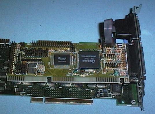
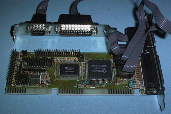
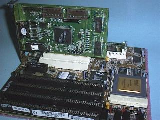
The bottom card is an MCA card, the top card is an ISA bus card
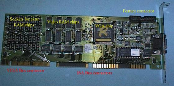
The IBM AT introduced a 16 bit data bus and the expansion slots had to handle 16 data bits. The industry wanted to be able to use existing 8-bit cards, so the new "AT" slot had to be designed to be backward compatible with the PC slots. The AT extension connector was added to the end of the 62 pin edge connector of the original 8-bit bus slot. This extension is a 36 pin edge connector. This bus slot was later given the name Industry Standard Architecture (ISA) and has survived to this day. One important aspect of this bus was that IBM never made any specification about bus speeds.
In the original 6MHz IBM AT, and the subsequent 8MHz version, the bus simply ran along at the same speed as the CPU. It was not surprising that as clone vendors started looking for a marketing edge over IBM, they simply kept the bus running at the CPU speed as they boosted speeds to 10MHz, 12MHz, and even faster. This lead to problems with users starting to run into problems. Boards that ran fine in a 6 or 8 MHz computer were not reliable in faster ones. The problem was especially severe with network cards. It turned out that they couldn't run at these higher clock speeds. The industry eventually settled on 8MHz as the standard maximum clock speed and the name Industry Standard Architecture.
One answer was to put the system memory on a local bus with the processor on the system board. The memory could be connected directly to the processors data bus and have no buffer devices between it and the processor. This way it could be 32 bits wide and accessed at the processors clock speed. At this stage in the development of RAM technology the industry was still using DIL package RAM chips of 256k bits or one Meg bit capacity and it took a lot of system board real estate to fit in more than a few megabytes of RAM.
Many companies decided to make special 32-bit expansion slots for proprietary memory boards that could be added later. This is where we can learn a lesson - many owners of computers with these system boards soon discover that they could not find these proprietary boards for their computers only a few months after they purchased the computer. Many manufacturers realised that a standard 32-bit bus was a better answer than many proprietary designs, and if it could run at the processor bus speed that would be even better.
Not only would the video system benefited from a faster/wider bus, faster hard drives and hard drive interfaces and network interface cards had outgrown the ISA bus. One solution was to design a faster bus for video and other components. Bringing the Bus Slot speed up to the then typical Bus Clock speed of 33 MHz, would provide a four-fold increase in data transfer rate. Double the width of the data bus from 16 to 32 bits, and the transfer rate could be up to eight times that of the ISA bus.
Some designers started by simply wiring video circuitry into the CPU bus on system boards. The system board already had a "local bus" between the processor and it's RAM and this could be extended to include the video interface. This provided speed gains, but at the cost of flexibility. If you wished to upgrade the Video System all you could do was to disable the video on the system board, and resort to an ISA card in a bus slot.
The next solution was a throwback to the proprietary 32-bit memory cards of the early 386 systems. Designers created their own unique solutions for local bus video slots. This approach left the buyer dependent on the original vendor to develop and offer new video options as technologies change and improve and at the rate of development of PC hardware, this usually never happened.
The problem was first solved by the Video Electronics Standards Association. This is the group that made sense out of the mayhem that occurred when vendors tried to go beyond IBM's original specification for VGA. When you wanted to run a system at higher than VGA's original specification of 640 by 480 you had to get drivers that worked with your application programs and hardware.
The VESA standards for Super VGA signal timing and resolutions sorted out much of this trouble. The committee set some basic goals for a local bus specification. It had to be low cost, based on existing technology and system chip sets as much as possible. It had to offer significantly higher performance, handling not only the present data transfer loads, but the additional traffic expected from even higher resolution displays and multimedia applications. It had to be an open standard, so anyone could use it, and it had to be software transparent, so you would not need to use any troublesome drivers. It also should be also extendible to handle future technology, such as the Pentium processor with its 64-bit data path.
The result was the VESA-Bus specification. This set forth the basic characteristics of the bus, such as mechanical, physical, timing, and protocol details. For maximum flexibility, it was designed in such a way that it could easily be added to ISA, EISA, or Micro Channel system boards. To keep the design simple, the committee designed the VESA-Bus as an extension of the internal bus used within the 80486 processor. As a result, the VESA-Bus could use the full address range of the 486 chip.
Many VESA slot equipped computer systems used a VESA, IDE/FDC/SPG interface card. The IDE interface on this card was the only part of the card that used the VESA-bus slot. The Floppy Disk Controller and the SPG functions still used the ISA portion of the slot.
Local Bus devices can be implemented with devices either integrated into the system board, or plugged into an expansion slot. The problem with integrated devices is the higher bus clock speeds push technology to its engineering limits. As the signals travel around the traces of printed circuit boards faster and faster, it is more and more difficult to maintain accurate timings. If an electrical signal is slowed too much on the way to its destination, then critical events may not take place at the correct instant, and processing crashes to a halt.
The faster the CPU runs, the smaller the load it can handle (the load on it's outputs). Sending a signal through an expansion slot rather than to a device located on the system board adds to the load on the bus. The VESA committee recommended only two VESA-Bus slots and two VESA-Bus devices (system board mounted devices) with a 33MHz (or slower) bus speed, one slot at 40MHz, and no slots at all for a 50MHz bus speed.
The PCI-Bus (Peripheral Component Interconnect) was originally designed to speed up the display of graphics on Intel-based personal computers, but the standard itself is processor independent and suitable for other hardware add-ons that require high bandwidth, including network, video and SCSI adaptors. PCI was developed by INTEL but it did take some time to get it to work reliably. By the middle of 1993 the VESA-Bus became firmly entrenched in the market place and almost all DOS computer systems had VESA-Bus slots as standard. The wide acceptance of local bus technology only took a few months and by default, VESA-Bus become the first Local Bus standard.
For a while, many people in the computer industry saw a local-bus war between the two competing local-bus standards (VESA-Bus and PCI-Bus) but in reality they were not in the same battlefield. The PCI and VESA Local-Busses did basically the same thing - both speed up PC computers by letting peripherals like graphics adaptors and hard disk controllers run at up to 33MHz, instead of the 8MHz that the ISA-Bus limited them to. The similarity breaks down when we start talking about how the two designs work.
The VESA-Bus bypassed the ISA bus by using the same bus the CPU is connected to it's RAM memory by and so it was relatively cheap and easy for system and peripheral makers to implement. Intel's PCI-Bus on the other hand, was a whole new bus, in much the same way the EISA and MCA busses were. The PCI bus gave only a slight speed improvement when used with 486 based systems, but it was far ahead when used with the Pentium chip.
The PCl-Bus uses three elegant techniques to resolve local bus problems. The first, known as reflective wave signalling, reduces the amount of electrical amplification required on the signal paths and thus reduces noise and loading problems. The second is multiplexing. Multiplexing allows two different signals to use the same electrical path, reducing the number of pins required for peripheral chips and lowering manufacturing costs. The third is a protocol letting the PCl controller receive specific configuration information from the PCl devices themselves. Intel did not defined a standard adaptor connector for the bus, leaving that job up to a PCl-Bus special-interest group who settled on the white 112 pin connector.
Other computer manufacturers are also using the PCI-Bus in there computer platforms with Digital Equipment Corp. (DEC) with their Alpha RISC-based systems, and Hewlett-Packard and SUN Microsystems all including PCI-Bus slots in there products. Intel licensed its patents on the PCI Bus free of royalties to all who wished to use it.
By adopting an established industry standard the manufacturers of the other computer platforms are ensuring lower costs and more options for both users and developers who are no longer locked into their own proprietary options. The wide range of cards that have followed the use of the PCI-Bus on PC systems are available for the first time to users of other hardware. All that should be required is alternative driver software for the various platforms.
Many combinations of the various buses that have been available over the years are possible and some system board manufacturers produced boards with combinations of ISA, EISA, MCA, VESA and PCI-Bus. This was to allow users to make use of older exotic cards such as SCSI controllers and hardware cache boards in upgraded equipment.
Most system boards available today still have two ISA bus slots but there are PCI bus slot only boards, and EISA and PCI only boards available.
| Bus type | Bus data width | Bus speed | Data transfer rate |
|---|---|---|---|
| PC/XT | 8 bits | 4.7 - 8 MHz | 3.25 (Mbits/Sec) |
| ISA | 16 bits | 8 MHz | 6.5 (Mbits/Sec) |
| EISA | 32 bits | 8 MHz | 32 (Mbits/Sec) |
| MCA | 32 bits | 8 MHz | 20 (Mbits/Sec) |
| VESA | 32 bits | 33 MHz to 50 MHz | 132 (Mbits/Sec) and above |
| PCI | 32 bits | 33 MHz | 132 (Mbits/Sec) |
This memory is referred to as AGP Memory. AGP in theory allows a peak data transfer rate of up to 528 Mbytes/second between the PC's main memory and the AGP graphics accelerator, compared to a transfer rate of only 132 Mbytes/second attainable by today's PCI bus. Doubts exist about this claim because this figure is the whole bandwidth of main memory and it has to be shared with CPU and other devices. AGP may never be able to get a throughput of 528 MB/s, but the trend to 100MHz bus speeds will speed main memory transfers and make this more likely.
Like most other modern PC developments, the chipset has to provide services for the AGP bus, in particular, the function to map the 'AGP memory' to normal main memory. Intel calls this GART (Graphics Address Remapping Table). This means the Video Interface can use some of the System Memory rather than having dedicated Video RAM on the card.
The benefits AGP is offering:
Software Considerations
Unfortunately, getting an AGP board plus an AGP graphic accelerator won't be enough to take advantage of AGP's new performance. The operating system has to take care of particularly the DIME/GART part of the AGP benefits. The Operating System has to provide main memory for the AGP RAM. This is achieved via DirectDraw in Windows98 and Windows NT 5.
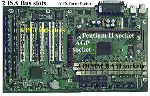
Example of a Pentium II System Board with an AGP socket
| Back to the opening index | Book two index |