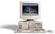
The Pentium Classic incorporates 3·1 million transistors (nearly triple the number in a 486), a 64-bit internal and external Data bus, separate built-in caches for data and instructions, a rebuilt floating-point unit (FPU), and a "superscalar" architecture that lets it process two instructions per clock cycle. The Address bus of the Pentium is still 32 bit as this gives enough memory access for the foreseeable future.
MMX technology provides the processor with 57 new instructions to implement a technique called Single Instruction, Multiple Data (SIMD) to reduce complex operations to a single step instruction. MMX (Muti-Media Extensions) target graphic generation and signal processing tasks such as bit mapping audio and video information to accelerate graphics, multimedia and communications processing. Applications must be written to use these new instructions and so we will see a gradual introduction of MMX aware software.
In an attempt to reduce heat dissipation the MMX desktop processors require two operating voltages. The I/O circuitry requires a 3·3 volt source and the "core" operates at 2·8 volt. Any source voltage outside the range of 3·1 to 3·6 volt, and any "core" voltage outside the range of 2·7 to 2·9 will cause the MMX Pentium processors to run at the wrong frequency. This means for optimum performance the MMX Pentium processors require System Boards that support dual CPU voltage selection, not a common feature in older Pentium System Boards.
Some System Boards will also require a BIOS upgrade and this will be a problem in many cases. The manufacturing life expectancy of most system boards is about six months and when a board is obsolete many manufacturers, or their agents, are no longer interested in supporting it.
Intels Pentium Pro (P6)
This processor has a built in (on-chip) 256K, 512K or 1Meg Level 2 cache, on the processor itself and uses a very large oblong socket called Socket 8. The chip has 5·5 million devices inside the core and a further 15·5 million devices in the smallest on-chip cache. The largest Cache has about 62 million devices inside. This chip was introduced in 1995.
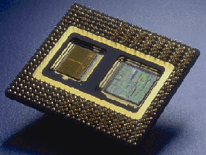
In the picture below, you can see quite clearly how the Pentium Pro processor is made in two parts, one part is the actual processor core the other is the built in level two cache. You can also see the new socket configuration that is required.
A picture of the Pentium Pro Processor showing the pin configuration
Intels Pentium II , the Klamath
This processor is packaged in a very different package called the Single Edge Contact (S.E.C.) package, with a single edge connector, instead of the multiple pins used in the PGA packages. This connector is called Slot 1.
This version of the Pentium II was introduced late in 1997 and is available at operating speeds of 233 MHz up to 300 MHz. The Klamath has an on-chip Cache that operates at half the Processor internal operating speed.
Pentium II vs Pentium Pro
The Pentium Pro is aimed at a different market segment to the newer Pentium II. The Pentium Pro has a weakness with 16 bit code, such as Windows 3·x or Windows 95, but performs very well when used with Windows NT and other advanced Server operating systems. The Pentium II's advantages over the Pentium Pro are the additional L1 cache, segment cache registers and MMX extensions.
Except for the larger L1 cache the other two features do not improve the Pentium II in high end server environments. Important advantages of the older Pentium Pro is the 8 fold larger cache able area of 4 GByte instead of the 512 MByte of the Pentium II, the ability to run in up to quad CPU configurations (Pentium II can only work in dual CPU), and operation of the on-chip L2 cache at the processor speed. The Pentium Pro is also available with on-chip cache as large as 1 Megabyte.
Intels Deschutes
Pentium II processors operating at 333, 350 and 400 MHz are given the name Deschutes. The 350 and 400 MHz versions are designed to operate with a 100 MHz External Clock, also referred to as a 100 MHz "front side bus".
The Celeron
This may be an attempt by Intel to put an end to the use of Socket 7, and hence upset AMD and Cyrix/IBM who are continuing to design new processors around this socket. The first Celeron released about April 1998, operated at 266 MHz and had no integrated (built-in on the chip assembly) Level 2 Cache. The Leon Processor uses a Single Edge Processor package (SEPP) similar to the SEC (also called Slot 1) used by the other Pentium II Processors. Both the SEPP and SEC socket configurations are a 242-contact socket, the only difference seems to be the retention mechanism and the heat sink provisions. The Celeron does not need the huge heat sink required by the other members of the Pentium II family and so has a simpler retention mechanism.
By June 1998 Intel had available a 300 MHz Celeron without an integrated Level 2 Cache, and by September they had another 300 MHz version (the 300A), and a 333 MHz version, with a 128 KByte Level 2 Cache on the chip. Intel plan to release a "very cheap" Celeron chip that will use a new socket rather than the Slot one used by the other Pentium II processors. It sounds like this socket will be new and nothing like the exiting socket seven.
The next developments from Intel will be the Xeon which will also use the Pentium II core with a second level cache of either 512K or 1Meg, that runs at the processor core speed. They will be available in 400 and 450 MHz versions, will use a new 330 connector Slot 2, and will have a 36 bit address bus, giving it access to a maximum of 64GByte of RAM !. The package for the Xeon is about twice as high as the earlier Pentium II processors, and has extensive on-board heat monitoring. After the Xeon we will see the Katmai, operating at 450 and 500 MHz and having an enhanced MMX2 instruction set, and then the Tanner and Merced Processors.
Supply Voltages
The 60 and 66Mhz versions of the Pentium operated on a 5 volt supply but the 75, 90, 100, 120, 133, 150, 166, and 200 MHz versions of the Pentium Classic use a 3·3 Volt supply. A suffix on some of the higher speed Pentium chips indicates the operating voltage range and these are "S" (standard) = 3·135 to 3·6 and "V" (voltage regulator enhanced) = 3·4 to 3·6 volt. Some Pentium System Boards made during 1996/7 have a Voltage Regulator Module (VRM) socket and this was provided to cater for future developments in processors, a feature that was never made use of.
The latest trend is to use two supply voltages to the processor chip, 3·3 volt to the I/O interface circuitry and between 2·1 and 2·9 volt to the "core" of the chip. This technique was introduced with the Pentium MMX processors. Older System Boards do not provide the split CPU power supply and so can't be used with the latest range of Pentium processors.
Pentium Processor Sockets.
The first Pentium processors, the 60 and 66Mhz chips used a large Pin Grid Array socket (PGA) with 296 pins, called Socket 4, and the 75MHz Pentium's introduced a new Staggered Pin Grid Array socket (SPGA), called Socket 5, with 320 pins. This socket was used for the 75, 90, 100 and 120 MHz Pentium's. The 133 to 200 MHz Pentium Classic and Pentium MMX use Socket 7 with 321 pins.
Advantages of the Pentium MMX over the Pentium Classic
In addition to the MMX instructions the Pentium MMX (P55C) chips have a larger Level one Cache (increased from 16K to 32K) and improved Pipeline Architecture to improve performance of existing applications. These changes have resulted in a performance increase for existing business applications of 5% to 15%. Existing graphics and communications applications should see a performance increase of 10% to 20% due to these changes.
As software manufacturers write new applications and optimize and recompile their existing applications to make use of the MMX instructions, we can expect performance increases of between 25% and 400%. MMX processors will not replace the modern accelerated 2-D and 3-D video cards. MMX on its own is not a graphics acceleration solution.
Summary of MMX features
- Doubling of the L1 Caches, 16KB Data and 16 KB Instruction Cache
- The Data Cache is now 4 Way Set Associative - only 2 Way Set Associative in Pentium Classic
- Double the number of the Write Buffers, now 4 instead of 2
- A new Branch Prediction Unit, taken from the more advanced Pentium Pro
- Implementation of a Return Stack (first done in the Cyrix/IBM 6x86)
- Increase of the U and V Pipelines by one step
- Improvement of the Parallel Processing Ability of the two Pipelines
- The MMX instruction set with the ability to pair up two MMX instructions in one go, hence 2 SIMD instructions can be processed with 16 byte data in one Clock Cycle
- new split voltage technology, 2·8 V for CPU core, 3·3 V for CPU I/O interface (lower heat dissipation)
Bus speeds
When we talk about a 100 MHz processor we are talking about the Core (internal) operating speed of that chip. There are two more clock speeds we have to look at as well.
The External Clock speed is the speed of the clock signal supplied to the processor, and it is also the speed at which the Processor accesses the RAM memory. Intel is now using the term Front Side Bus to refer to this clock speed.
The Bus Clock speed is the access speed of the external Bus slots and with the PCI Bus, it is usually 33 MHz. The Advanced Graphics Port operates at 66 to 133 MHz.
Most Pentium System Boards can supply External Clock speeds of 50, 55, 60, 66, and 75 MHz, and some can supply 83 Mhz. The original PCI bus was limited by definition to 33MHz but the PCI standard 2.1 requires System Boards to operate reliably with a PCI bus speed of up to 40MHz.
The PCI Bus usually operates at half the External Clock speed but problems may be caused when the PCI Bus is run at half 75 MHz or 83 MHz. System Boards with the higher Bus clock speeds will have an option of running the PCI Bus at a lower speed.
The Pentium and Pentium clone processors have two programming pins that set the Processors Core Clock speed multiplier value. These two pins at present usually provide multiplier values of 1·5, 2·0, 2·5 and 3·0. We will see future processors use these pins for other multiplier values, the AMD K5 chip has a fixed multiplier and does not use these pins.
The following page, The clock speeds, bus speeds and multiplier values for some of the Processors available in early 1998.
By experimenting with the Bus clock speed and the multiplier values, we can run processors at higher speeds than they are designed for, and with higher PCI Bus speeds. This process is called Over Clocking and can achieve remarkable increases in performance. It can also make the system unreliable or at the worst, destroy the processor by over heating.
100Mhz external clock speed.
The 80486 Processor operated with an External Clock speed of 25 to 40 MHz, and this was also the Clock Speed at which the Processor accessed the RAM. The Pentium Processor was introduced with an External Clock speed or either 60 or 66 MHz. This gave an significant increase in the speed at which RAM was accessed. This speed has been pushed to 75 and 83MHz by some processors but this sometimes leads to RAM access problems, due to problems with timing in the RAM devices, and the Chipset.
Early in 1998 Intel released the BX chipset and this device has support for an External Clock speed of up to 100 MHz. Intel also introduced the name Front Side Bus for the bus between the Processor and the RAM. This term was introduced to draw a difference between the external bus between the Processor and the RAM and the on-chip bus, between the processor core and the on-chip Cache. This internal bus has been called the Back Side Bus. Remember Intels Klamath, and Deschutes Pentium II Processors all have a Level 2 Cache on the chip.
Will the newer Intel compatible chips operate in older System Boards ?
Bitter experience over the years has shown that unless a particular System Board was produced after a more advanced Processor was introduced, and hence it was tested with that device and has jumpers for that device, most System Boards can't be upgraded with a newer Processor without a change to the BIOS. Modern System Boards use a "soft" BIOS called a Flash ROM and can be upgraded for newer Processors, if a later version of the BIOS is made available by the board manufacturer.
Intel Pentium compatible chips produced by other companies
AMD processors
NexGen merged with AMD and produced the K5 chip, a Pentium clone, and the K6, a Pentium MMX clone. The AMD-K6 has been made in operating speeds of 166MHz to 300MHz.
AMD now have a K6-2 (also called K6-3D) Processor with 3D enhancements. These chips will soon be available with operating speeds up to 450 MHz, have on-chip level 2 cache, operate with 100 MHz bus speeds and still use the old Socket 7. This chip will be followed by a K6plus2 (also called K6+3D) chip and there will be an AMD-K7 device that will use the Slot 1 used by the Pentium II.
An image of the AMD K5 processor chip
IBM and Cyrix processors
IBM produces the chips designed by Cyrix and they both market Pentium clones under the same names. The first chip they produced was the 6x86 (also called the M1). This chip was then produced as the 6x86L, operating with a spilt power supply, like the Pentium MMX. The 6x86 P200+ (internal clock speed 150 MHz) versions required a System Board that could support a 75 MHz bus speed. This chip has been replaced by the 6x86MX with MMX extensions (also called the M2).
An image of the Cyrix 6x86 Processor chip
The IDT WinChip C6
Another recent entry into the processor market is the company Integrated Device Technologies (IDT). They have released a chip called the WinChip C6, but not much has been seen of it yet. The company is using the marketing slogan, the first Microprocessor Chip optimized for Microsoft Windows business applications.
An image of the IDT WinChip C6 Processor
The PowerPC
A consortium consisting of IBM, Motorola, Apple, SUN Microsystems and others tried to take the lead in the next generation of microcomputers by building machines around the PowerPC line of reduced-instruction-set computing (RISC) microprocessors jointly developed by Motorola and IBM. The consortium of companies hoped their Chip would draw many followers away for alternatives such as Intel's Pentium processor running Microsoft's Windows NT operating system. IBM shipped the first PowerPC version of its RS/6000 work-station in 1994, and Apple had PowerPC Apple Mackintoshes (PowerMac) on sale by mid 1994.
Operating system support for the PowerPC was slow in developing and most software companies were slow in developing native versions of applications for the PowerPC platform. IBM offered versions of its OS/2 2·1 and AIX (a flavor of Unix) operating systems on its first PowerPC microcomputers, and Apple supplied versions of it operating systems. None of the operating systems offered achieved much market share and as of early 1998, it looks as though the PowerPC is almost dead, and Apple Computer, the only serious user of the platform, could be in trouble.
Internet Television and very low cost PC's
In the USA this class of PC is also called the sub $1000 PC. PC hardware could undergo great change in the next two or three years with the traditional hardware giving way to simple but powerful computers, far different to what we know now. Traditional hardware will continue to be used for Servers and high performance Work Stations, but the majority of Home Computers may well be Internet Televisions, or "Set Top Box's". Processor manufacturers are gearing up for this change, some to cater for the new concept, some to counter it's spread. Cyrix is the first to make an advanced processor to counter the attack on the PC's dominance with its MediaGX processor and companion chip.
New terms
Backside bus - A special internal microprocessor bus that connects the CPU to a Level 2 cache inside the processor package. Typically, a backside bus runs at a faster clock speed than the frontside bus that connects the CPU to the ouside world and the main memory. For example, the Pentium Pro microprocessor actually consists of two pieces of silicon on a common substrate. One "chip" contains the CPU and the primary (L1) cache, and the other "chip" contains the secondary (L2) cache. A backside bus connects the two chips at the same clock rate as the CPU itself. The earlier Pentium II chips ran the cache (and the backside bus) at half the processor speed. In contrast, the frontside bus runs at only a fraction of the CPU clock speed.
Frontside bus - The bus within a microprocessor that connects the CPU with the ouside world and the main memory. In contrast, a Backside bus connects the CPU to a Level 2 cache inside the processor.
Copyright © Phil. Storr, last updated 26th December 1998