
3.6 What Does This Have To Do With Computers, Anyway?
Although there is a tenuous relationship between boolean functions and boolean expressions in programming languages like C or Pascal, it is fair to wonder why we're spending so much time on this material. However, the relationship between boolean logic and computer systems is much stronger than it first appears. There is a one-to-one relationship between boolean functions and electronic circuits. Electrical engineers who design CPUs and other computer related circuits need to be intimately familiar with this stuff. Even if you never intend to design your own electronic circuits, understanding this relationship is important if you want to make the most of any computer system.
3.6.1 Correspondence Between Electronic Circuits and Boolean Functions
There is a one-to-one correspondence between an electrical circuits and boolean functions. For any boolean function you can design an electronic circuit and vice versa. Since boolean functions only require the AND, OR, and NOT boolean operators1, we can construct any electronic circuit using these operations exclusively. The boolean AND, OR, and NOT functions correspond to the following electronic circuits, the AND, OR, and inverter (NOT) gates (see Figure 3.13).
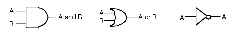
Figure 3.13 AND, OR, and Inverter (NOT) Gates
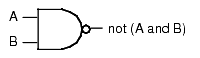
One interesting fact is that you only need a single gate type to implement any electronic circuit. This gate is the NAND gate, shown in Figure 3.14.
To prove that we can construct any boolean function using only NAND gates, we need only show how to build an inverter (NOT), an AND gate, and an OR gate from a NAND (since we can create any boolean function using only AND, NOT, and OR). Building an inverter is easy, just connect the two inputs together (see Figure 3.15).
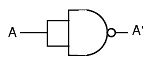
Figure 3.15 Inverter Built from a NAND Gate
Once we can build an inverter, building an AND gate is easy - just invert the output of a NAND gate. After all, NOT (NOT (A AND B)) is equivalent to A AND B (see Figure 3.16). Of course, this takes two NAND gates to construct a single AND gate, but no one said that circuits constructed only with NAND gates would be optimal, only that it is possible.
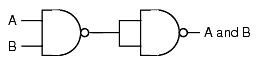
Figure 3.16 Constructing an AND Gate From Two NAND Gates
The remaining gate we need to synthesize is the logical-OR gate. We can easily construct an OR gate from NAND gates by applying DeMorgan's theorems.
(A or B)'				=	A' and B'					DeMorgan's Theorem.

A or B				=	(A' and B')'					Invert both sides of the equation.

A or B				=	A' nand B'					Definition of NAND operation.
By applying these transformations, you get the circuit in Figure 3.17.
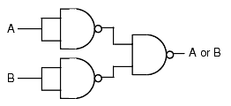
Figure 3.17 Constructing an OR Gate from NAND Gates
Now you might be wondering why we would even bother with this. After all, why not just use logical AND, OR, and inverter gates directly? There are two reasons for this. First, NAND gates are generally less expensive to build than other gates. Second, it is also much easier to build up complex integrated circuits from the same basic building blocks than it is to construct an integrated circuit using different basic gates.
Note, by the way, that it is possible to construct any logic circuit using only NOR gates2. The correspondence between NAND and NOR logic is orthogonal to the correspondence between the two canonical forms appearing in this chapter (sum of minterms vs. product of maxterms). While NOR logic is useful for many circuits, most electronic designs use NAND logic.
3.6.2 Combinatorial Circuits
A combinatorial circuit is a system containing basic boolean operations (AND, OR, NOT), some inputs, and a set of outputs. Since each output corresponds to an individual logic function, a combinatorial circuit often implements several different boolean functions. It is very important that you remember this fact - each output represents a different boolean function.
A computer's CPU is built up from various combinatorial circuits. For example, you can implement an addition circuit using boolean functions. Suppose you have two one-bit numbers, A and B. You can produce the one-bit sum and the one-bit carry of this addition using the two boolean functions:
	S 	=	AB' + A'B					Sum of A and B.

	C 	=	AB					Carry from addition of A and B.
These two boolean functions implement a half-adder. Electrical engineers call it a half adder because it adds two bits together but cannot add in a carry from a previous operation. A full adder adds three one-bit inputs (two bits plus a carry from a previous addition) and produces two outputs: the sum and the carry. The two logic equations for a full adder are
	S 			=	A'B'Cin + A'BCin' + AB'Cin' + ABCin

	Cout			=	AB + ACin + BCin
Although these logic equations only produce a single bit result (ignoring the carry), it is easy to construct an n-bit sum by combining adder circuits (see Figure 3.18). So, as this example clearly illustrates, we can use logic functions to implement arithmetic and boolean operations.
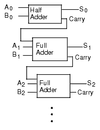
Figure 3.18 Building an N-Bit Adder Using Half and Full Adders
Another common combinatorial circuit is the seven-segment decoder. This is a combinatorial circuit that accepts four inputs and determines which of the segments on a seven-segment LED display should be on (logic one) or off (logic zero). Since a seven segment display contains seven output values (one for each segment), there will be seven logic functions associated with the display (segment zero through segment six). See Figure 3.19 for the segment assignments. Figure 3.20 shows the segment assignments for each of the ten decimal values.
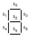
Figure 3.19 Seven Segment Display
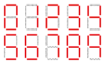
Figure 3.20 Seven Segment Values for "0" Through "9"
The four inputs to each of these seven boolean functions are the four bits from a binary number in the range 0..9. Let D be the H.O. bit of this number and A be the L.O. bit of this number. Each logic function should produce a one (segment on) for a given input if that particular segment should be illuminated. For example S4 (segment four) should be on for binary values 0000, 0010, 0110, and 1000. For each value that illuminates a segment, you will have one minterm in the logic equation:
S4 = D'C'B'A' + D'C'BA' + D'CBA' + DC'B'A'.S0, as a second example, is on for values zero, two, three, five, six, seven, eight, and nine. Therefore, the logic function for S0 is
S0 = D'C'B'A' + D'C'BA' + D'C'BA + D'CB'A + D'CBA' + D'CBA + DC'B'A' + DC'B'AYou can generate the other five logic functions in a similar fashion.
Decoder circuits are among the more important circuits in computer system design. They provide the ability to recognize (or `decode') a string of bits. One very common use for a decoder is memory expansion. For example, suppose a system designer wishes to install four (identical) 256 MByte memory modules in a system to bring the total to one gigabyte of RAM. These 256 MByte memory modules have 28 address lines (A0..A27) assuming each memory module is eight bits wide (228 x 8 bits is 256 MBytes)3. Unfortunately, if the system designer hooked up those four memory modules to the CPU's address bus they would all respond to the same addresses on the bus. Pandemonium would result. To correct this problem, we need to select each memory module when a different set of addresses appear on the address bus. By adding a chip enable line to each of the memory modules and using a two-input, four-output decoder circuit, we can easily do this. See Figure 3.21 for the details.
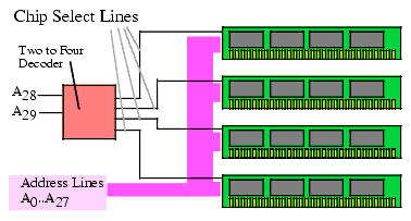
Figure 3.21 Adding Four 256 MByte Memory Modules to a System
The two-line to four-line decoder circuit in Figure 3.21 actually incorporates four different logic functions, one function for each of the outputs. Assume the inputs are A and B (A=A28 and B=A29) then the four output functions have the following (simple) equations:
		Q0 = A' B'

		Q1 = A B'

		Q2 = A' B

		Q3 = A B
Following standard electronic circuit notation, these equations use "Q" to denote an output (electronic designers use "Q" for output rather than "O" because "Q" looks somewhat like an "O" and is more easily differentiated from zero). Also note that most circuit designers use active low logic for decoders and chip enables. This means that they enable a circuit with a low input value (zero) and disable the circuit with a high input value (one). Likewise, the output lines of a decoder chip are normally high and go low when the inputs select a given output line. This means that the equations above really need to be inverted for real-world examples. We'll ignore this issue here and use positive (or active high) logic4.
Another big use for decoding circuits is to decode a byte in memory that represents a machine instruction in order to activate the corresponding circuitry to perform whatever tasks the instruction requires. We'll cover this subject in much greater depth in a later chapter, but a simple example at this point will provide another solid example for using decoders.
Most modern (Von Neumann) computer systems represent machine instructions via values in memory. To execute an instruction the CPU fetches a value from memory, decodes that value, and the does the appropriate activity the instruction specifies. Obviously, the CPU uses decoding circuitry to decode the instruction. To see how this is done, let's create a very simple CPU with a very simple instruction set. Figure 3.22 provides the instruction format (that is, it specifies all the numeric codes) for our simple CPU.
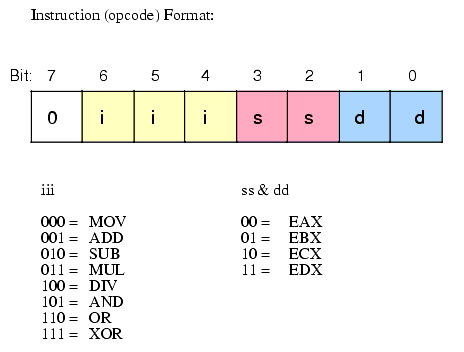
Figure 3.22 Instruction (opcode) Format for a Very Simple CPU
To determine the eight-bit operation code (opcode) for a given instruction, the first thing you do is choose the instruction you want to encode. Let's pick "MOV( EAX, EBX);" as our simple example. To convert this instruction to its numeric equivalent we must first look up the value for MOV in the iii table above; the corresponding value is 000. Therefore, we must substitute 000 for iii in the opcode byte.
Second, we consider our source operand. The source operand is EAX, whose encoding in the source operand table (ss & dd) is 00. Therefore, we substitute 00 for ss in the instruction opcode.
Next, we need to convert the destination operand to its numeric equivalent. Once again, we look up the value for this operand in the ss & dd table. The destination operand is EBX and it's value is 01. So we substitute 01 for dd in our opcode byte. Assembling these three fields into the opcode byte (a packed data type), we obtain the following bit value: %00000001. Therefore, the numeric value $1 is the value for the "MOV( EAX, EBX);" instruction (see Figure 3.23).
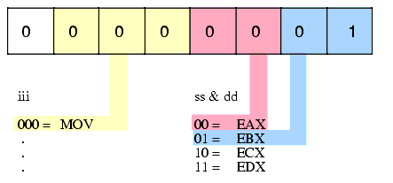
Figure 3.23 Encoding the MOV( EAX, EBX ); Instruction
As another example, consider the "AND( EDX, ECX);" instruction. For this instruction the iii field is %101, the ss field is %11, and the dd field is %10. This yields the opcode %01011110 or $5E. You may easily create other opcodes for our simple instruction set using this same technique.
- Warning: please do not come to the conclusion that these encodings apply to the 80x86 instruction set. The encodings in this examples are highly simplified in order to demonstrate instruction decoding. They do not correspond to any real-life CPU, and they especially don't apply to the x86 family.
In these past few examples we were actually encoding the instructions. Of course, the real purpose of this exercise is to discover how the CPU can use a decoder circuit to decode these instructions and execute them at run time. A typical set of decoder circuits for this might look like that in Figure 3.24:
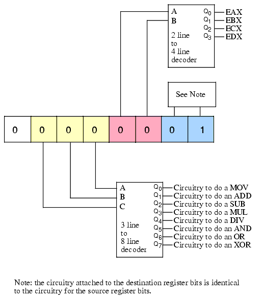
Figure 3.24 Decoding Simple Machine Instructions
Notice how this circuit uses three separate decoders to decode the individual fields of the opcode. This is much less complex than creating a seven-line to 128-line decoder to decode each individual opcode. Of course, all that the circuit above will do is tell you which instruction and what operands a given opcode specifies. To actually execute this instruction you must supply additional circuitry to select the source and destination operands from an array of registers and act accordingly upon those operands. Such circuitry is beyond the scope of this chapter, so we'll save the juicy details for later.
Combinatorial circuits are the basis for many components of a basic computer system. You can construct circuits for addition, subtraction, comparison, multiplication, division, and many other operations using combinatorial logic.
3.6.3 Sequential and Clocked Logic
One major problem with combinatorial logic is that it is memoryless. In theory, all logic function outputs depend only on the current inputs. Any change in the input values is immediately reflected in the outputs5. Unfortunately, computers need the ability to remember the results of past computations. This is the domain of sequential or clocked logic.
A memory cell is an electronic circuit that remembers an input value after the removal of that input value. The most basic memory unit is the set/reset flip-flop. You can construct an SR flip-flop using two NAND gates, as shown in Figure 3.25.
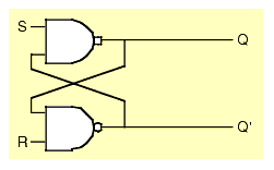
Figure 3.25 Set/Reset Flip Flop Constructed from NAND Gates
The S and R inputs are normally high. If you temporarily set the S input to zero and then bring it back to one (toggle the S input), this forces the Q output to one. Likewise, if you toggle the R input from one to zero back to one, this sets the Q output to zero. The Q' input is generally the inverse of the Q output.
Note that if both S and R are one, then the Q output depends upon Q. That is, whatever Q happens to be, the top NAND gate continues to output that value. If Q was originally one, then there are two ones as inputs to the bottom flip-flop (Q nand R). This produces an output of zero (Q'). Therefore, the two inputs to the top NAND gate are zero and one. This produces the value one as an output (matching the original value for Q).
If the original value for Q was zero, then the inputs to the bottom NAND gate are Q=0 and R=1. Therefore, the output of this NAND gate is one. The inputs to the top NAND gate, therefore, are S=1 and Q'=1. This produces a zero output, the original value of Q.
Suppose Q is zero, S is zero and R is one. This sets the two inputs to the top flip-flop to one and zero, forcing the output (Q) to one. Returning S to the high state does not change the output at all. You can obtain this same result if Q is one, S is zero, and R is one. Again, this produces an output value of one. This value remains one even when S switches from zero to one. Therefore, toggling the S input from one to zero and then back to one produces a one on the output (i.e., sets the flip-flop). The same idea applies to the R input, except it forces the Q output to zero rather than to one.
There is one catch to this circuit. It does not operate properly if you set both the S and R inputs to zero simultaneously. This forces both the Q and Q' outputs to one (which is logically inconsistent). Whichever input remains zero the longest determines the final state of the flip-flop. A flip-flop operating in this mode is said to be unstable.
The only problem with the S/R flip-flop is that you must use separate inputs to remember a zero or a one value. A memory cell would be more valuable to us if we could specify the data value to remember on one input and provide a clock input to latch the input value. This type of flip-flop, the D flip-flop (for data) uses the circuit in Figure 3.26.
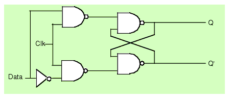
Figure 3.26 Implementing a D flip-flop with NAND Gates
Assuming you fix the Q and Q' outputs to either 0/1 or 1/0, sending a clock pulse that goes from zero to one back to zero will copy the D input to the Q output. It will also copy D' to Q'. The exercises at the end of this topic section will expect you to describe this operation in detail, so study this diagram carefully.
Although remembering a single bit is often important, in most computer systems you will want to remember a group of bits. You can remember a sequence of bits by combining several D flip-flops in parallel. Concatenating flip-flops to store an n-bit value forms a register. The electronic schematic in Figure 3.27 shows how to build an eight-bit register from a set of D flip-flops.
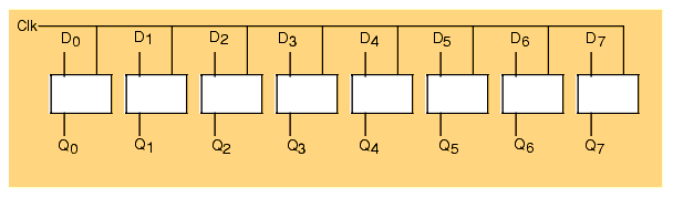
Figure 3.27 An Eight-bit Register Implemented with Eight D Flip-flops
Note that the eight D flip-flops use a common clock line. This diagram does not show the Q' outputs on the flip-flops since they are rarely required in a register.
D flip-flops are useful for building many sequential circuits above and beyond simple registers. For example, you can build a shift register that shifts the bits one position to the left on each clock pulse. A four-bit shift register appears in Figure 3.28.
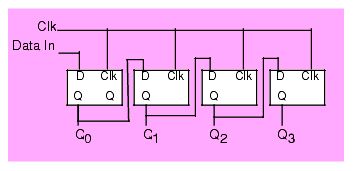
Figure 3.28 A Four-bit Shift Register Built from D Flip-flops
You can even build a counter, that counts the number of times the clock toggles from one to zero and back to one using flip-flops. The circuit in Figure 3.29 implements a four bit counter using D flip-flops.
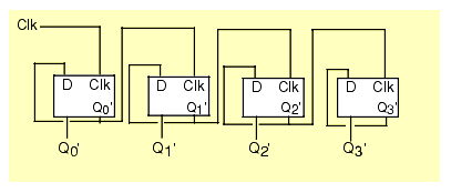
Figure 3.29 Four-bit Counter Built from D Flip-flops
Surprisingly, you can build an entire CPU with combinatorial circuits and only a few additional sequential circuits beyond these. For example, you can build a simple state machine known as a sequencer by combining a counter and a decoder as shown in Figure 3.30. For each cycle of the clock this sequencer activates one of its output lines. Those lines, in turn, may control other circuitry. By "firing" these circuits on each of the 16 output lines of the decoder, we can control the order in which these 16 different circuits accomplish their tasks. This is a fundamental need in a CPU since we often need to control the sequence of various operations (for example, it wouldn't be a good thing if the "ADD( EAX, EBX);" instruction stored the result into EBX before fetching the source operand from EAX (or EBX). A simple sequencer such as this one can tell the CPU when to fetch the first operand, when to fetch the second operand, when to add them together, and when to store the result away. But we're getting a little ahead of ourselves, we'll discuss this in greater detail in a later chapter.
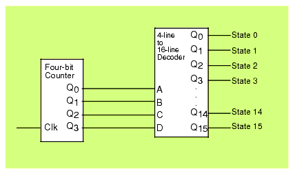
Figure 3.30 A Simple 16-State Sequencer
3.7 Okay, What Does It Have To Do With Programming, Then?
Once you have registers, counters, and shift registers, you can build state machines. The implementation of an algorithm in hardware using state machines is well beyond the scope of this text. However, one important point must be made with respect to such circuitry - any algorithm you can implement in software you can also implement directly in hardware. This suggests that boolean logic is the basis for computation on all modern computer systems. Any program you can write, you can specify as a sequence of boolean equations.
Of course, it is much easier to specify a solution to a programming problem using languages like Pascal, C, or even assembly language than it is to specify the solution using boolean equations. Therefore, it is unlikely that you would ever implement an entire program using a set of state machines and other logic circuitry. Nevertheless, there are times when a hardware implementation is better. A hardware solution can be one, two, three, or more orders of magnitude faster than an equivalent software solution. Therefore, some time critical operations may require a hardware solution.
A more interesting fact is that the converse of the above statement is also true. Not only can you implement all software functions in hardware, but it is also possible to implement all hardware functions in software. This is an important revelation because many operations you would normally implement in hardware are much cheaper to implement using software on a microprocessor. Indeed, this is a primary use of assembly language in modern systems - to inexpensively replace a complex electronic circuit. It is often possible to replace many tens or hundreds of dollars of electronic components with a single $5 microcomputer chip. The whole field of embedded systems deals with this very problem. Embedded systems are computer systems embedded in other products. For example, most microwave ovens, TV sets, video games, CD players, and other consumer devices contain one or more complete computer systems whose sole purpose is to replace a complex hardware design. Engineers use computers for this purpose because they are less expensive and easier to design with than traditional electronic circuitry.
You can easily design software that reads switches (input variables) and turns on motors, LEDs or lights, locks or unlocks a door, etc. (output functions). To write such software, you will need an understanding of boolean functions and how to implement such functions in software.
Of course, there is one other reason for studying boolean functions, even if you never intend to write software intended for an embedded system or write software that manipulates real-world devices. Many high level languages process boolean expressions (e.g., those expressions that control an IF statement or WHILE loop). By applying transformations like DeMorgan's theorems or a mapping optimization it is often possible to improve the performance of high level language code. Therefore, studying boolean functions is important even if you never intend to design an electronic circuit. It can help you write better code in a traditional programming language.
For example, suppose you have the following statement in Pascal:
if ((x=y) and (a <> b)) or ((x=y) and (c <= d)) then SomeStmt;You can use the distributive law to simplify this to:
if ((x=y) and ((a <> b) or (c <= d)) then SomeStmt;Likewise, we can use DeMorgan's theorem to reduce
while (not((a=b) and (c=d)) do Something;while (a <> b) or (c <> d) do Something;
So as you can see, understanding a little boolean algebra can actually help you write better software.
3.8 Putting It All Together
A good understanding of boolean algebra and digital design is absolutely necessary for anyone who wants to understand the internal operation of a CPU. As an added bonus, programmers who understand digital design can write better assembly language (and high level language) programs. This chapter provides a basic introduction to boolean algebra and digital circuit design. Although a detailed knowledge of this material isn't necessary if you simply want to write assembly language programs, this knowledge will help explain why Intel chose to implement instructions in certain ways; questions that will undoubtedly arise as we begin to look at the low-level implementation of the CPU.
This chapter is not, by any means, a complete treatment of this subject. If you're interested in learning more about boolean algebra and digital circuit design, there are dozens and dozens of texts on this subject available. Since this is a text on assembly language programming, we cannot afford to spend additional time on this subject; please see one of these other texts for more information.
1We know this is true because these are the only operators that appear within canonical forms.
2NOR is NOT (A OR B).
3Actually, most memory modules are wider than eight bits, so a real 256 MByte memory module will have fewer than 28 address lines, but we will ignore this technicality in this example.
4Electronic circuits often use active low logic because the circuits that employ them typically require fewer transistors to implement.
5In practice, there is a short propagation delay between a change in the inputs and the corresponding outputs in any electronic implementation of a boolean function.
|